Heterogeneous Integrated Chip Fabrication
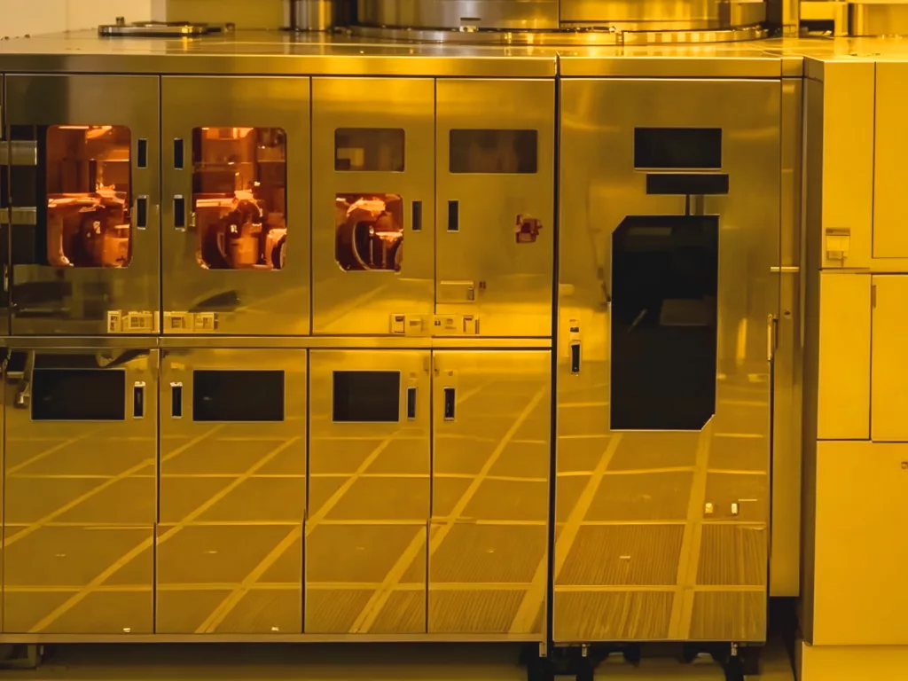
- Full-process fabrication of silicon passive structures and III-V active devices: photolithography, ICP etching, oxide/silicon dielectric deposition and patterning, metal electrode patterning/deposition/lift-off
- Equipment: DUV stepper, ICP etcher, LPCVD/PECVD, ion implantation, e-beam evaporation
- Key specs: min linewidth 150 nm, overlay ±50 nm; waveguide sidewall verticality 89°, surface roughness 5 nm; active diode average resistance ~5 Ω, single-device output 10 mW