

From Single Devices to CMOS Imaging: How Emerging Optoelectronic Materials Cross the Engineering Validation Gap
For decades, photodetector research has been evaluated against a relatively well-defined set of performance metrics: higher responsivity, lower dark current, higher specific detectivity, faster response speed, and broader spec...
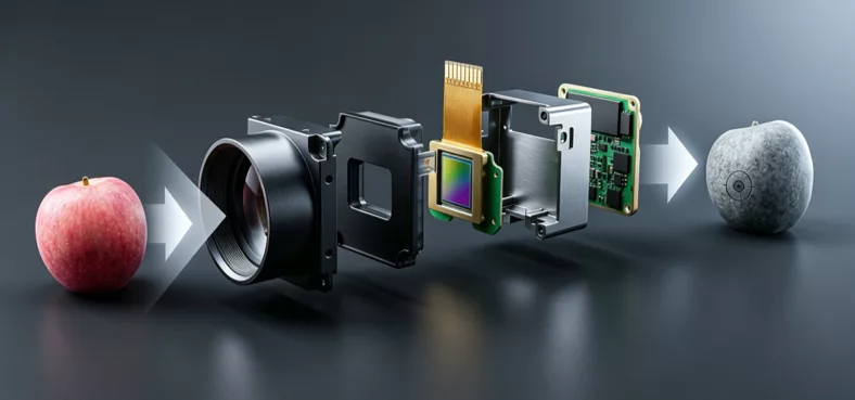
Why Colloidal Quantum Dots Could Enable the Scalable Adoption of SWIR Imaging
Short-Wave Infrared (SWIR) imaging is widely recognized as one of the most promising sensing technologies beyond conventional visible vision. By capturing material-specific optical information, SWIR enables non-destructive ins...
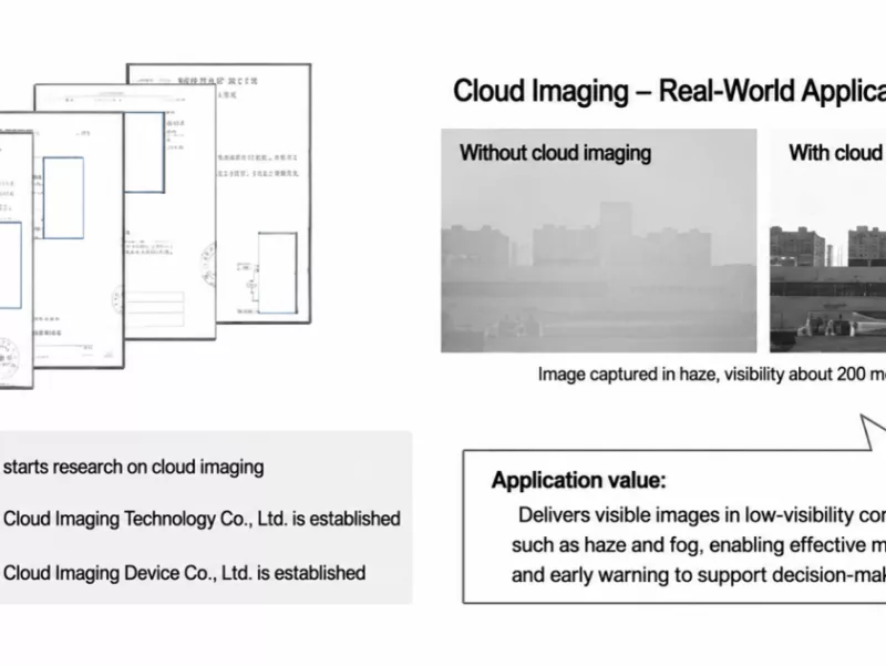
From Flip-Chip Bonding to Monolithic Integration – How Quantum Dot Technology Is Unlocking Mass Production of Industrial SWIR Imaging
Short-wave infrared (SWIR, 900–1700 nm) imaging has long occupied a critical position in high-end machine vision due to its unique ability to reveal material properties beyond the visible spectrum. However, its industrial-scal...