
From Flip-Chip Bonding to Monolithic Integration – How Quantum Dot Technology Is Unlocking Mass Production of Industrial SWIR Imaging
Short-wave infrared (SWIR, 900–1700 nm) imaging has long occupied a critical position in high-end machine vision due to its unique ability to reveal material properties beyond the visible spectrum. However, its industrial-scale adoption has been constrained by the high cost and manufacturing complexity of traditional III-V semiconductor technologies.
With the maturation of colloidal quantum dot (CQD) technology, a new generation of monolithic SWIR photodetectors is emerging—offering a scalable and cost-effective alternative for industrial inspection, semiconductor metrology, photovoltaic testing, laser analysis, security imaging, precision agriculture, and automotive vision systems.
01 Spectral Value: Why SWIR Is Essential for Industrial Imaging
SWIR imaging bridges the gap between visible and thermal imaging by enabling material-level contrast and subsurface penetration that neither modality can provide.
In industrial environments, SWIR imaging addresses three core challenges:
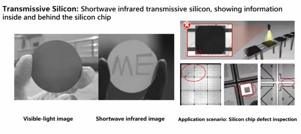
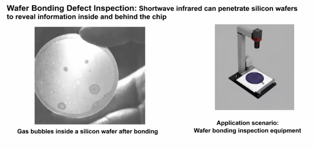
▼ Silicon Subsurface Inspection
Silicon is transparent to wavelengths above ~1100 nm due to its 1.12 eV bandgap.
This enables SWIR cameras to see through silicon wafers, making it possible to detect:
- Internal micro-cracks
- Alignment marks
- Subsurface defects
This capability is essential for wafer-level packaging (WLP) and 3D integration inspection in semiconductor manufacturing.
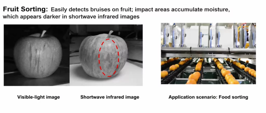
▼ Material Fingerprint Identification
Many materials exhibit distinct absorption features in the SWIR band, including:
- Water and moisture
- Polymers and plastics
- Organic compounds
- Food and pharmaceutical materials
Unlike RGB imaging, which captures appearance, SWIR imaging reveals material composition.
This enables high-contrast sorting and inspection in:
- Food quality control
- Plastic recycling
- Pharmaceutical powder inspection
- Agricultural moisture analysis


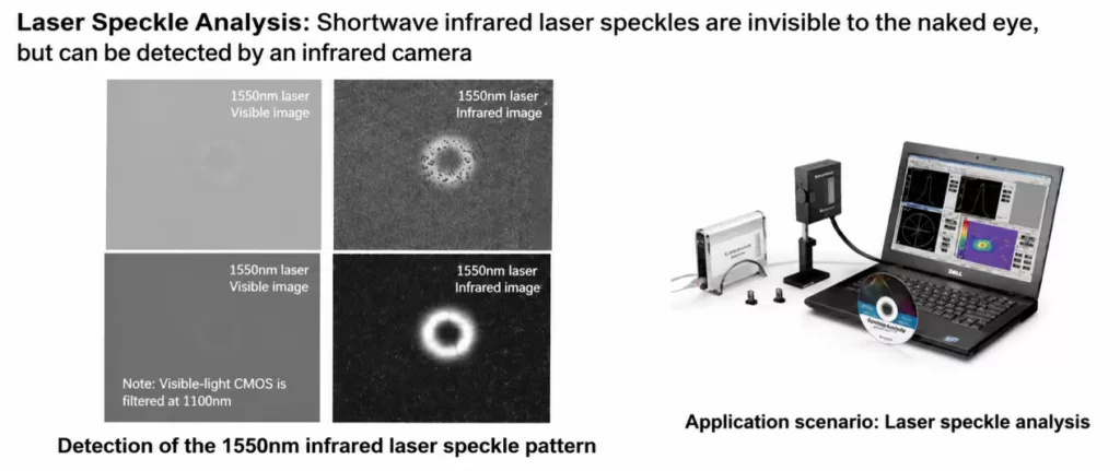
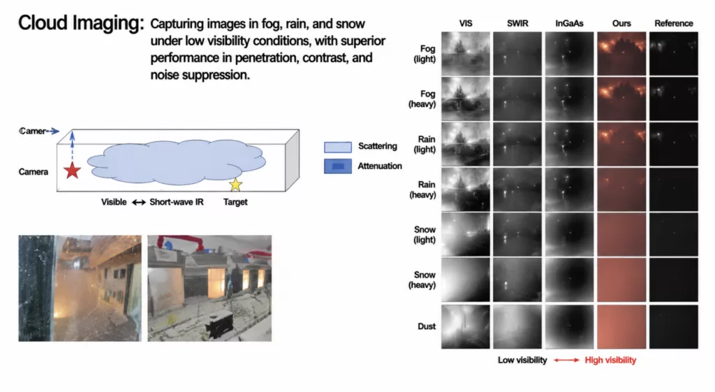
▼ Imaging in Smoke, Haze, and Harsh Environments
Compared to visible light, SWIR wavelengths experience significantly reduced Rayleigh scattering.
This enables stable imaging in:
- Smoke and dust environments
- Laser processing and welding monitoring
- Long-range surveillance and inspection
02 Technology Foundation: From Bandgap Engineering to InGaAs Systems
SWIR detection relies on converting low-energy photons into electrical signals through appropriate bandgap materials.
- Silicon (Si): ideal for visible and NIR, but loses sensitivity beyond ~1000 nm
- InGaAs: dominant SWIR material (900–1700 nm), with high quantum efficiency (>80%) and low dark current
However, InGaAs-based detectors face fundamental manufacturing constraints:
▼ Flip-Chip Heterogeneous Integration
Conventional InGaAs sensors require flip-chip bonding between InP-based photodiode arrays and silicon ROICs using indium bump interconnects.
Each pixel requires precise micro-scale alignment.
For megapixel arrays, this results in:
- Extremely complex assembly processes
- Lower manufacturing yield
- Limited pixel pitch scaling (typically 10–15 µm)
- Restricted resolution scalability (commonly VGA-class systems)
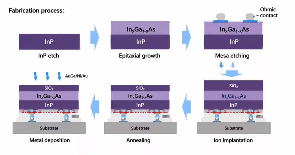
▼ Wafer Size Limitation
InP substrates are typically 3–4 inches, compared to 8–12 inch silicon wafers.
This limits economies of scale and significantly increases cost per device.
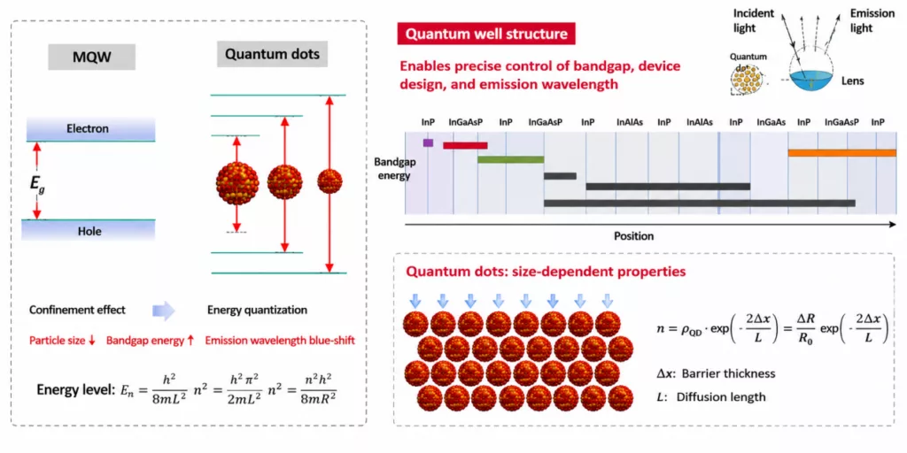
03 Technological Shift: Quantum Dot (CQD) Photodetection Mechanism
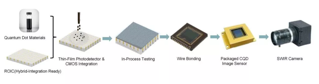
Colloidal quantum dot (CQD) technology introduces a fundamentally different approach to SWIR detection using solution-processed nanocrystals (e.g., PbS quantum dots).
This enables a monolithic SWIR imaging architecture, eliminating key limitations of III-V systems.
▼ Monolithic Integration via Solution Processing
CQD materials can be directly deposited onto CMOS ROICs via spin-coating, similar to photoresist processing.
This enables:
- No InP substrate required
- No flip-chip bonding
- Full compatibility with standard CMOS fabrication lines
- Scalable wafer-level production
▼ Tunable Spectral Response
By controlling quantum dot size (quantum confinement effect), the spectral response can be precisely engineered.
This enables coverage of:
- 900–1700 nm (InGaAs-equivalent range)
- Extended SWIR beyond 2000 nm (e-SWIR)
All within a single material platform.
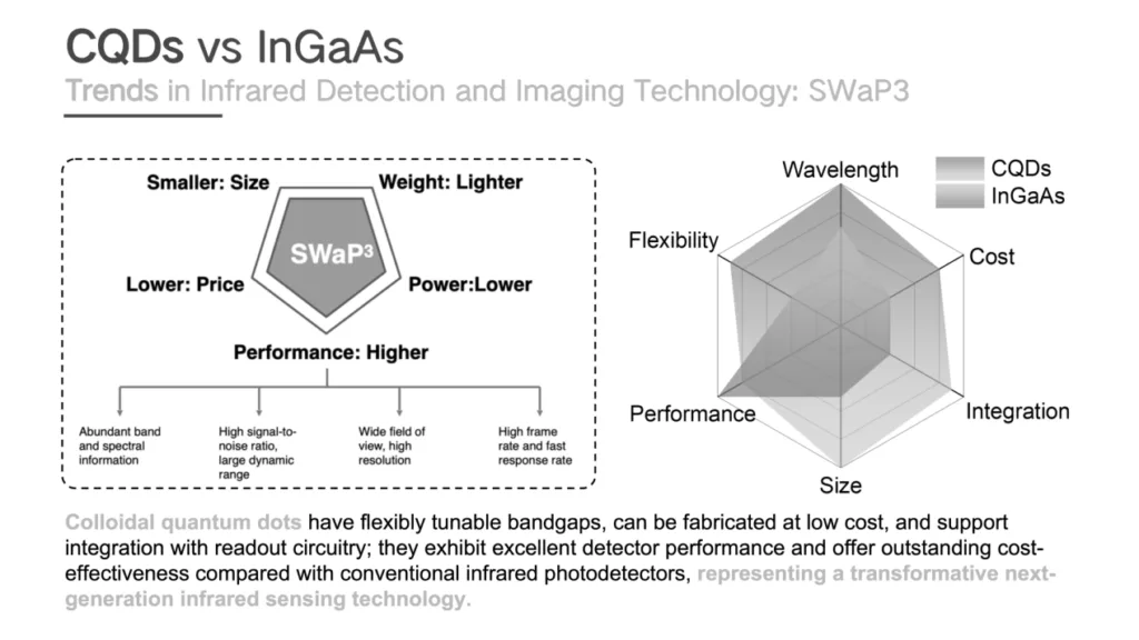
▼ High Resolution and SWaP-C Advantage
Eliminating bump bonding enables significantly smaller pixel pitches (<2 µm), supporting:
- Full HD (1080p) and 4K SWIR imaging
- Compact system integration
- Lower power consumption
- Reduced system cost
This directly aligns with SWaP-C (Size, Weight, Power, and Cost) requirements for next-generation vision systems.
Market Outlook
According to industry forecasts (e.g., Yole Group), the SWIR imaging market is expected to grow at a CAGR of approximately 28%, driven by advancements in semiconductor inspection, industrial automation, and machine vision systems.
Conclusion
The evolution from flip-chip bonded InGaAs sensors to monolithic quantum dot SWIR imaging technology represents a fundamental shift in infrared photonics.
By enabling:
- Wafer-scale manufacturing
- Tunable spectral engineering
- CMOS compatibility
- High-resolution scalable imaging
CQD technology is redefining the economics and accessibility of SWIR imaging.
In the long term, its greatest value lies not only in performance improvement, but in structural cost disruption, unlocking large-scale adoption across industrial, scientific, and emerging consumer vision applications.