

Nature | Professor Tang Jiang’s Team at Huazhong University of Science and Technology Achieves a New Breakthrough in Monolithic, In-Situ Aqueous Integration!
Inspired by biomineralization, Professor Tang Jiang’s team at Huazhong University of Science and Technology (HUST) has proposed a monolithic and in-situ integration (MISI) strategy. Using a room-temperature aqueous-phase process, the team directly grows electronic-grade lead sulfide (PbS) thin films on a readout integrated circuit (ROIC), enabling high-performance infrared detection and imaging. This strategy offers a new materials-growth and monolithic-integration route for infrared imaging chips with a low thermal budget and scalability.
The 640 × 512 CMOS readout integrated circuit supplied by InRight Infrared has appeared in Nature for the first time.
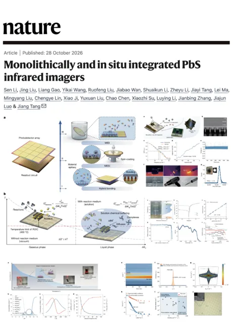
The paper, entitled “Monolithically and in situ integrated PbS infrared imagers,” was published in Nature. InRight Infrared provided the 640 × 512 CMOS ROIC and readout-circuit design support for this study, helping the team complete monolithic, in-situ integration and validate array-level imaging.
Conventional infrared imaging chips typically require the detector array and readout circuit to be fabricated separately and then integrated through bonding or other processes. A major challenge in bringing emerging infrared materials to large-format imaging is to grow high-quality photosensitive materials directly on a fully fabricated ROIC while also meeting constraints on thermal budget, carrier transport, and pixel-to-pixel uniformity.
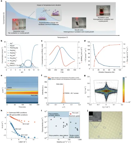
To address this challenge, the team used a Pb–OH coordination system to regulate the release of growth-active species. The reaction was precisely controlled within a narrow pH window of 11.2–11.3. Combined with high-precision temperature control and precision vibration isolation, this approach stabilized supersaturation at the solid–liquid interface, promoting heterogeneous nucleation at the substrate interface while suppressing homogeneous nucleation in solution.
The resulting quasi-single-crystalline PbS thin films combine excellent electronic transport properties with large-area uniformity:
The films exhibit a carrier concentration of approximately 2 × 10¹⁵ cm⁻³ and a Hall mobility of 124 cm²·V⁻¹·s⁻¹, with wafer-scale thickness uniformity of ±2.1%. These properties provide a materials foundation for the subsequent fabrication of high-performance detectors and array integration.
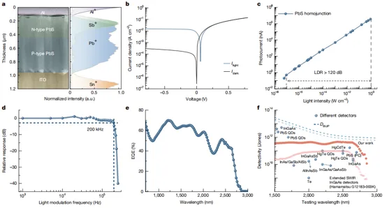
Building on this, the team introduced antimony (Sb) dopants to form an n-type PbS layer and constructed vertical PbS p–n homojunction photodiodes, achieving key optoelectronic performance advances:
- Room-temperature specific detectivity: ~4.4 × 10¹¹ Jones (at 2.5 μm)
- External quantum efficiency: >40% (0.7–2.6 μm wavelength range)
- Linear dynamic range: >120 dB (measured under 1300 nm illumination)
- −3 dB bandwidth under self-powered operation: ~200 kHz
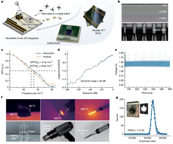
The research team then directly grew a PbS detector layer on the 640 × 512 CMOS ROIC supplied by InRight Infrared, forming an infrared focal-plane array (FPA) with a 15 μm pixel pitch. By integrating photosensitive-material growth and silicon-based readout-circuit integration into a single process flow, this approach enabled the team to evaluate array uniformity and imaging performance across more than 320,000 pixels.
The resulting imaging device achieved:
- Photo-response non-uniformity (PRNU): 5.05%
- Imaging dynamic range: ~62 dB
Without cooling or external illumination, the imager could capture infrared images of heat sources at temperatures ranging from 80 to 600 °C. In transmission-imaging experiments, it could also resolve details of leaf veins, further demonstrating the technology’s potential to advance from single-device characterization to array-level imaging.
The study also demonstrated the feasibility of extending the MISI strategy to flexible readout-circuit platforms and lead selenide (PbSe) material systems, offering a new research direction for the monolithic integration of a broader range of emerging optoelectronic materials with silicon-based circuits.
Why Does Research on Emerging Optoelectronic Materials Require Platform-Level Engineering Validation?
Moving emerging optoelectronic materials from the laboratory to imaging applications requires progress across multiple stages, including materials preparation, device fabrication, array integration, development of supporting modules and systems, and optoelectronic performance testing.
A single-pixel device can provide an initial validation of a material’s photoresponse and device performance. However, assessing its engineering potential requires a focal-plane imaging system to further evaluate the following:
• Can consistent responses be maintained across pixels?
• Are the materials and device processes suitable for large-area fabrication?
• Can PRNU, noise, and defective pixels be controlled?
• Can the images support algorithm analysis and real-world applications?
To address these needs, the monolithic-integration and sensing-validation platform provided by Inright Infrared enables research teams to translate material-level advantages into device performance, array metrics, and system-level image quality. It also helps identify critical issues in materials and processes more efficiently during engineering development, allowing researchers to focus more of their efforts on materials innovation, new optoelectronic detection mechanisms, and fundamental scientific questions.