
Why Colloidal Quantum Dots Could Enable the Scalable Adoption of SWIR Imaging
Short-Wave Infrared (SWIR) imaging is widely recognized as one of the most promising sensing technologies beyond conventional visible vision. By capturing material-specific optical information, SWIR enables non-destructive inspection, material identification, and imaging in challenging environments, making it increasingly valuable for semiconductor inspection, machine vision, laser communications, agricultural sorting, and security monitoring.
Despite these advantages, SWIR technology has historically remained confined to research instrumentation, high-end industrial inspection, and defense-related applications. While its sensing capabilities far exceed those of conventional visible-light imaging in many scenarios, widespread adoption has been constrained by cost and manufacturing complexity.
In recent years, Colloidal Quantum Dot Short-Wave Infrared (CQD-SWIR) technology has emerged as a promising alternative. By integrating quantum dot photodetectors with mature CMOS manufacturing processes, CQD-SWIR offers a new pathway toward high-resolution, cost-effective, and scalable SWIR image sensors.
01 SWIR Is Not Thermal Imaging
A Material-Aware Extension of Machine Vision
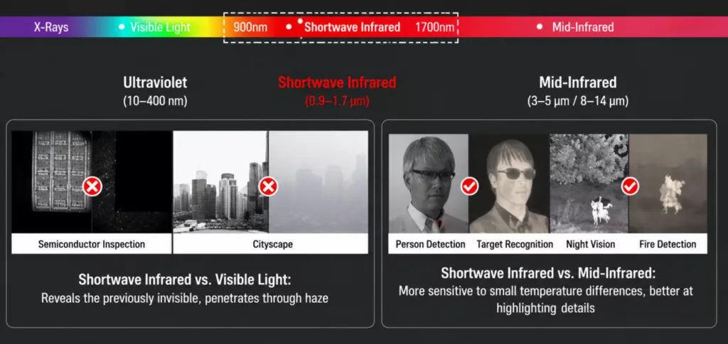
When infrared imaging is mentioned, thermal cameras are often the first technology that comes to mind. However, SWIR imaging operates on a fundamentally different principle from Mid-Wave Infrared (MWIR) and Long-Wave Infrared (LWIR) thermal imaging systems.
MWIR and LWIR cameras primarily detect thermal radiation emitted by objects, allowing temperature distributions to be visualized. In contrast, SWIR sensors capture reflected light and exploit the unique absorption and reflectance characteristics of materials at specific wavelengths.
In other words, SWIR focuses not on temperature, but on the intrinsic optical properties of materials.
This capability enables a range of applications that are difficult or impossible to achieve using conventional visible-light cameras.
▼ Non-Destructive Inspection of Silicon and Semiconductor Devices
Silicon, the foundational material of the semiconductor industry, has a bandgap of approximately 1.12 eV, corresponding to a wavelength of about 1100 nm.
At wavelengths longer than 1100 nm, silicon becomes increasingly transparent. As a result, SWIR cameras can visualize internal structures hidden beneath the surface of silicon wafers and semiconductor packages.
This unique characteristic makes SWIR an important tool for:
- Wafer crack detection
- Semiconductor defect inspection
- Package structure analysis
- Bonding quality evaluation
- Failure analysis
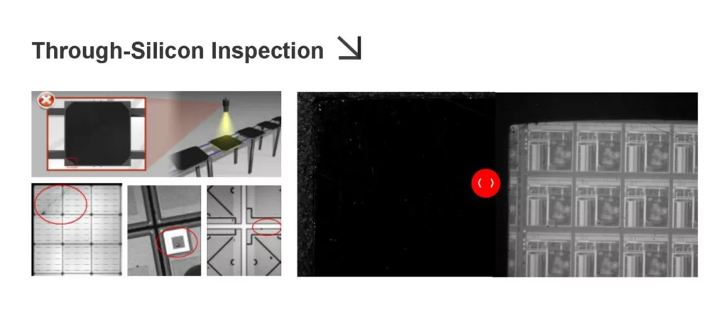
Compared with conventional inspection methods, SWIR enables non-contact and non-destructive observation of internal structures while improving inspection efficiency and reliability.
▼ Moisture Detection and Agricultural Quality Assessment
Water molecules exhibit strong absorption features near 1450 nm and 1940 nm.
When SWIR light interacts with water-containing materials, a significant portion of the incident photons is absorbed, creating strong image contrast related to moisture distribution.
This property supports a wide range of applications, including:
- Fruit ripeness evaluation
- Agricultural sorting
- Food quality inspection
- Moisture-content analysis
- Internal bruise detection
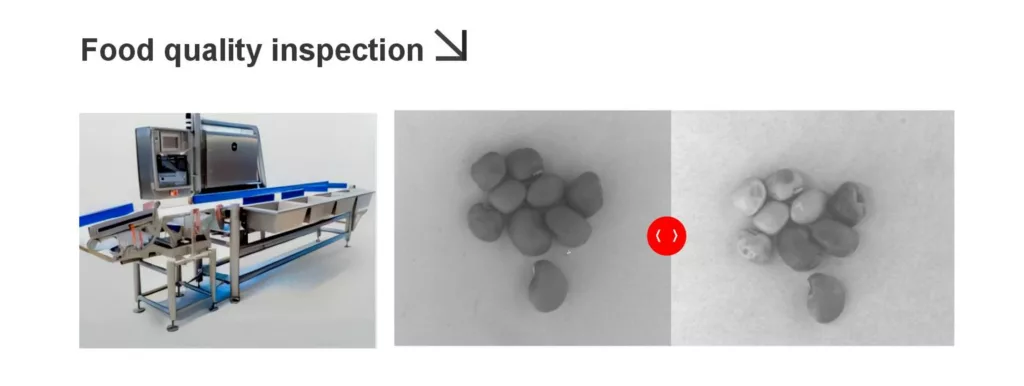
Defects that are invisible to the human eye can often be readily identified through SWIR imaging.
▼ Material Identification and Intelligent Sorting
Many materials that appear visually similar under visible light exhibit significantly different spectral reflectance signatures in the SWIR region. Examples include:
- Plastics and polymer materials
- Dark packaging materials
- Textile fibers
- Chemical powders
- Recyclable materials

These spectral differences provide valuable features for machine learning and artificial intelligence algorithms, making SWIR a powerful tool for:
- Material classification
- Intelligent sorting
- Multispectral inspection
- Industrial quality control
▼ Imaging in Smoke, Haze, and Challenging Environments
According to light-scattering theory, longer wavelengths experience reduced scattering when interacting with airborne particles.
Because SWIR wavelengths are significantly longer than visible wavelengths, SWIR imaging often delivers improved performance in environments containing light smoke, haze, water vapor, or aerosols.
This capability supports applications such as:
- Intelligent transportation systems
- Outdoor machine vision
- Security and surveillance
- Firefighting and emergency response
- Autonomous perception systems
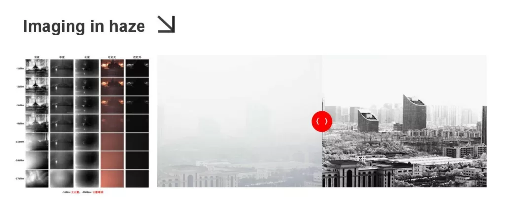
In challenging environmental conditions, SWIR can provide more stable and reliable imaging performance than conventional visible-light cameras.
02 What Are Colloidal Quantum Dots?
Why Could They Transform SWIR Imaging?
Today’s SWIR market is primarily dominated by InGaAs detector technology. While InGaAs sensors offer excellent responsivity, reliability, and mature performance, they typically rely on separate fabrication of detector arrays and readout integrated circuits (ROICs), followed by hybrid integration through flip-chip bonding.
As resolution increases and pixel sizes continue to shrink, manufacturing complexity and system costs can rise significantly.
Colloidal Quantum Dots offer a fundamentally different approach.
CQDs are nanoscale semiconductor crystals whose electronic and optical properties are governed by quantum confinement effects. By precisely controlling particle size during synthesis, researchers can engineer the bandgap and tune the spectral response of the material, enabling customizable sensitivity across the SWIR spectrum.
Compared with conventional InGaAs materials, CQDs can be synthesized through low-temperature solution-based processes and are inherently compatible with mature CMOS manufacturing technologies. This compatibility creates opportunities for wafer-level manufacturing and large-scale production, making CQD-SWIR one of the most actively explored directions in next-generation infrared imaging.
However, the true significance of CQD-SWIR extends beyond the material itself. Its greatest potential lies in enabling a fundamentally different device architecture.
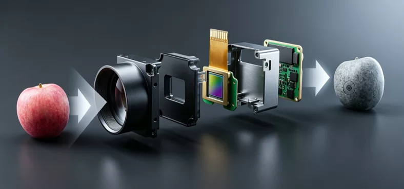
03 Monolithic Integration: A New Architecture for SWIR Sensors
▼ PbS Quantum Dot Photodetector Layer
In a CQD-SWIR sensor, a PbS quantum dot thin film can be directly deposited onto CMOS wafers during back-end semiconductor processing using scalable techniques such as:
- Spin coating
- Spray coating
- Blade coating
- Printing-based deposition
This layer is responsible for:
- Absorbing SWIR photons
- Generating photocarriers
- Performing photoelectric conversion
▼ CMOS Readout Integrated Circuit (ROIC)
The underlying CMOS circuitry provides:
- Charge readout
- Signal processing
- Pixel-array integration
- System-level functionality
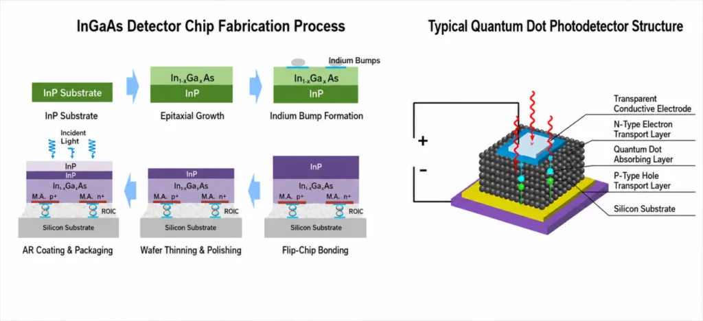
This architecture avoids the stringent lattice-matching requirements associated with conventional III-V semiconductor epitaxial growth while reducing dependence on costly hybrid integration processes.
As a result, CQD-SWIR offers a more cost-competitive path toward smaller pixel pitches and higher-resolution SWIR image sensors.
A Scalable Path Toward High-Resolution SWIR Imaging
The broader significance of CQD-SWIR lies in its potential to bring SWIR imaging closer to the manufacturing model that enabled the success of CMOS image sensors.
Over the past two decades, the rapid growth of the CMOS imaging industry has been driven by:
- Continuous pixel-size reduction
- Increasing image resolution
- Declining manufacturing costs
- High-volume wafer-level production
CQD-SWIR shares many of these characteristics through its compatibility with CMOS processes and monolithic integration strategies.
As quantum dot materials, device architectures, and wafer-level manufacturing technologies continue to mature, the cost of high-resolution SWIR sensors is expected to decrease significantly, opening the door to broader commercial adoption beyond traditional scientific and industrial markets.
04 From Research to Industrial Reality
While quantum dot SWIR technology has often been viewed as a laboratory-stage research topic, significant progress has recently been achieved in its practical implementation.
At InRight Tech, internally developed PbS quantum dot SWIR image sensors have achieved a 4-megapixel resolution (2048 × 2048) with a 5 μm pixel pitch, representing an important milestone in the advancement of high-resolution, small-pixel CQD-SWIR technology.
This achievement demonstrates not only the feasibility of high-performance multispectral imaging based on quantum dots, but also the long-term potential of scalable SWIR manufacturing.
As production processes continue to mature, CQD-SWIR technology is expected to unlock new opportunities across:
- Embodied AI and intelligent robotics
- Autonomous driving and advanced perception systems
- Industrial machine vision
- Multispectral and hyperspectral imaging
- On-chip spectroscopy
- Next-generation intelligent sensing platforms
Conclusion
SWIR imaging provides unique capabilities that extend far beyond conventional visible-light vision, enabling non-destructive inspection, moisture analysis, material identification, and enhanced imaging in challenging environments.
Although traditional InGaAs technology has established the foundation of the SWIR industry, its manufacturing complexity and cost structure have limited large-scale adoption.
By combining solution-processable quantum dot materials with mature CMOS manufacturing infrastructure, CQD-SWIR introduces a new pathway toward scalable, high-resolution, and cost-effective infrared imaging.
As the technology continues to evolve, colloidal quantum dots may play a pivotal role in transforming SWIR from a specialized sensing technology into a broadly deployed platform for next-generation intelligent vision systems.